
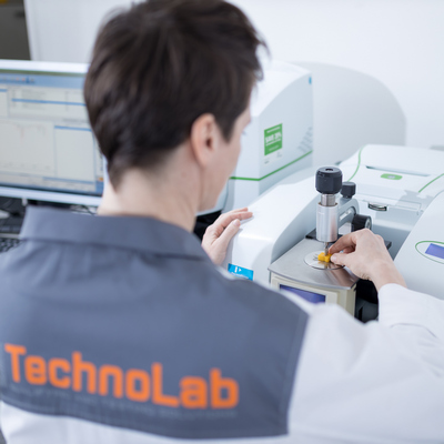
Failure Analysis – Advanced Testing and Diagnostics
Failure analysis is a critical aspect in the world of manufacturing and technology that deals with the identification, assessment and prevention of damage to materials, products or systems. This discipline plays a crucial role in ensuring the quality, safety and long-term reliability of a wide range of products, and the main objective of failure analysis is to understand the causes of damage and derive preventive measures. This ranges from small components to complex industrial systems. Through our advanced testing and diagnostics procedures, potential risks can be minimized and the service life of products extended.

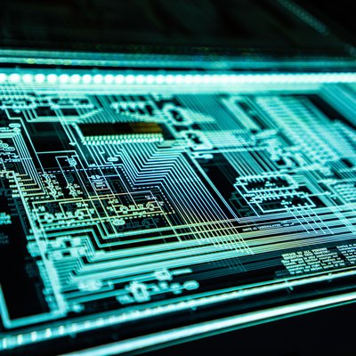
Optical inspection with microscope and microendoscope

Light microscopes with magnifications of 5x to 250x are used for magnified viewing and initial visual examination, the latter then for further examination of metallographic sections, for example. The examinations use reflected light, bright field or dark field analysis to inspect assemblies, record defect patterns or measure layer thicknesses.
In the case of mating contacts, inhomogeneities are examined or further results are visualized using a combined microsection analysis.
The aim is to make the damage roughly visible and to collect information for further analysis.
Basics according to IPC-A-610
- Bright field
- Dark field
- Interference contrast
- Polarization
- UV light
Laser topography
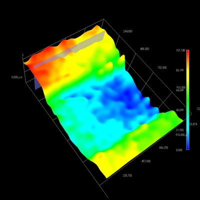
- optical surface scanning
- Roughness measurement
- Specimen size up to 300 x 300 mm
- Resolution up to 10 nm
Metallographic preparation techniques
Many damaged areas can only be identified using micrographs. The disadvantage here is that the parts to be examined are usually extracted from a larger part and then prepared, which results in a destructive examination.
The advantage here is that the defective parts are embedded in the casting during such examinations and therefore cracks, incorrect layer thicknesses, intermetallic zones, grain sizes, corrosion damage, inclusions, homogeneities and others can be determined and detected.
Examples of investigations are Layer thicknesses, inner layers of ceramic multilayer capacitors, inner layer connections of printed circuit boards, solder connections of components, plug connections, crimp connections, popcorning on semiconductors.
- Specimen dimension up to 160 x 30 mm grinding surface
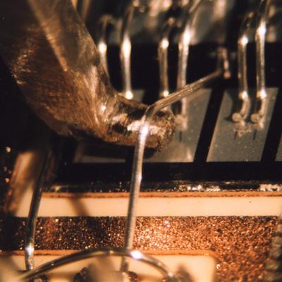
Dye and Pry Test
This test is used for a quick assessment of the quality of solder joints on BGA components to detect cracks or poor soldering quality and, if necessary, to optimize the process values in production. The advantage here is, for example, the simple, more cost-effective method compared to a ground joint preparation, in that a short-term result can be achieved without prior high preparation costs. The component is torn away from the surface of the assembly after the dye has been applied and dried and the poorly "infiltrated" solder joints can be seen from the penetrated dye.
- Detection of cracks (microcracks) in BGA solder joints
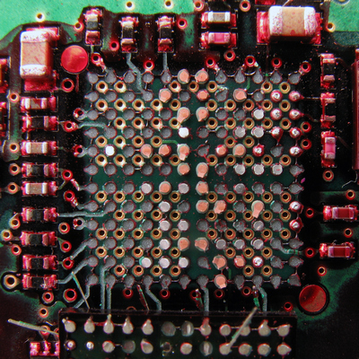
SEM (scanning electron microscopy) with EDX material analysis
SEM analysis is not only used for high-resolution and high-magnification imaging, but can also be used for material analysis in conjunction with an EDX detector. With SEM, surface structures are resolved very well and the element analysis can also be used to determine the materials or compositions of these in order to detect deposits, traces of corrosion, soiling, etc.
Layer thicknesses, whiskers, layer structures and the smallest cracks can also be detected here.
- SEM inspection + analysis by energy or wavelength dispersive X-ray spectroscopy (EDX/WDX)
X-ray and CT / laminography

The X-ray examination is a non-destructive examination that also uses 3D laminography / CT technology to detect processing or material defects (cavities, internally torn bond wires on ICs, condition of relay contacts, visualization of filling materials or in preparation for further examinations).
For example, the following are examined:
- Visualization of concealed solder joints
- Untersuchung von Anschlusskontakten
- Examination of connection contacts
- Solder bushings
Investigations are carried out in accordance with the following standards, among others:
- DIN EN 61191-6
- MIL 883 Meth. 2012
- AS6081
- IDEA-STD-1010
X-ray fluorescence (XRF/XRF)
- Qualitative and quantitative determination of the elemental composition and layer thickness determination of a sample
Fourier Transform Infrared Spectroscopy (FTIR)
We use FTIR analysis to examine very small areas for residues of organic substances that can cause corrosion of contacts or poor soldering results, for example.
Contamination on surfaces can be determined, for example to examine and localize the effects of auxiliary materials (e.g. cleaning fluids) used on machines in production. Basically, deposits, residues and even inclusions of materials that do not belong there can be determined.
Aging states of plastics (potting compounds, component sheathing, cable insulation) can also be measured, e.g. under the influence of heat or UV radiation (sun simulation)
- Identification of organic substances (polymers, adhesives, fluxes...)
Pull test
- Mechanical tests, such as tension, compression, bending, shear and pull tests, as well as the determination of insertion, extraction and retention forces.
Ionic contamination measurement (J-STD-0001 / IPC-TM-650)
- Detection of ionogenic contaminants (e.g. process residues from PCB production, flux residues, etc.) on assemblies
- Adaptation of the process to customer-specific requirements
CAF and SIR test
When qualifying printed circuit boards, they can be placed in an environment with a defined high level of moist heat and stored in this environment with an electrical voltage applied. An electrical voltage is applied either to the different prepeg layers or to the surface of neighboring conductor tracks.
When measuring the insulation cyclically, the insulation resistance decreases over time. The effect is caused by the growth of copper filaments. Depending on the test, this is referred to as CAF (Conductive Anodic Filament) or SIR (Surface Insulation Resistance). This is also referred to as accelerated service life testing.
Among other things, these tests are also used to detect or highlight contamination (process residues) or incorrect handling (fingerprints).
- CAF Test according to IPC-TM-650
Consulting
- Failure mechanisms of solder joints
- Failure mechanisms of components (e.g. ceramic capacitors)
- Failure mechanisms of printed circuit boards (keyword: black pad)
- Evidence reliability of test methods
- Evaluation of supplier agreements for technical relevance and feasibility
- Empirical determination of MTBF data